Key takeaways
- All five designs passed final schematic review; every original ERC report recorded zero errors and warnings.
- Verification covered exported connectivity, component ratings, tolerance calculations, temperature operating points and functional or behavioral simulations.
- The next step is to scale the evaluation to more complex circuits and test physical hardware.
Results
Five tasks, five final schematic passes
ProtoFlow completed five selected Easy schematic-design tasks adapted from PCBSchemaGen: a CAN transceiver, 60 V sensing divider, NTC temperature sensor, 3.3 V LDO supply and precision voltage reference. All five passed final review, with zero errors and warnings in their original ERC reports. Additional checks verified connectivity, component ratings, calculations and simulated behavior.
| Task | Function | Original ERC | Final schematic review | Functional evidence |
|---|---|---|---|---|
| 37 | CAN transceiver | 0 errors / 0 warnings | PASS | Connectivity and later functional-model checks |
| 01 | 60 V sense divider | 0 / 0 | PASS | Analytical tolerances and reported nominal simulation |
| 26 | NTC sensor + RC filter | 0 / 0 | PASS | Three manufacturer R–T operating-point runs |
| 05 | 12 V → 3.3 V LDO | 0 / 0 | PASS | Behavioral-model DC/startup/load checks |
| 33 | 5 V → 3.3 V reference | 0 / 0 | PASS | Surrogate sweeps; separate error allocation |
Method
Evaluation method
Each task began in a blank project and produced an editable schematic, netlist, BOM and engineering report. Interactive follow-up checks included model and fixture corrections; the results below describe the final reviewed designs. Review checked required pin memberships in all five saved exports and compared calculations with saved simulation data. Tasks were adapted from PCBSchemaGen_v2 revision e07c545f4c01a8026480b1093ee503a926ce2be5.
Task 37
CAN Transceiver: Connectivity and Functional Verification
The SN65HVD230DR interface uses a regulated 3.3 V supply, 100 nF bypass capacitor and 120 Ω endpoint termination across CANH/CANL. It assumes shared ground, 3.3 V MCU logic and a second termination elsewhere on the bus. Exported connectivity matched every required pin assignment.
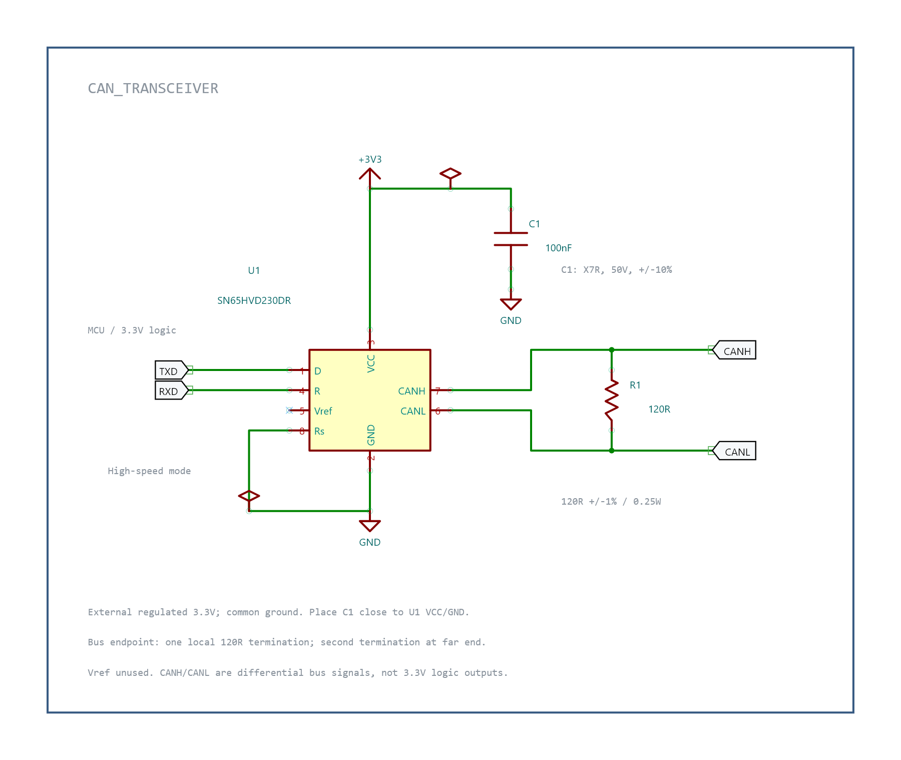
| Pin / component | Required connection |
|---|---|
| U1.1: D | TXD |
| U1.4: R | RXD |
| U1.3: VCC | +3V3 and C1.1 |
| U1.2: GND / U1.8: Rs | Ground |
| U1.7 / U1.6 | CANH / CANL |
| U1.5: Vref | Intentional no-connect |
| R1 | Across CANH and CANL |
| C1 | Across +3V3 and ground |
The termination is specified at ±1% and 0.25 W; the bypass capacitor is ±10%, X7R and 50 V. At a conservative 3.6 V differential, the termination dissipates approximately 0.109 W at its low-tolerance resistance. The final functional model passed loopback, standby release and reception from an externally driven dominant bus. A 1 ms run contained 1,280 samples; at approximately 40.4 µs, CANH = 2.50666 V and CANL = 0.79334 V, giving 1.71332 V differential. Recessive samples had approximately equal line voltages.
Task 01
Voltage Divider: Tolerance and Component Stress
A 180 kΩ / 10 kΩ divider scales 60 V to VSENSE. Both resistors are Viking ARG-series 0805 thin-film parts specified at ±0.1%. The adapted task required 3.10–3.30 V nominal output and a maximum of 3.30 V across initial resistor tolerances.
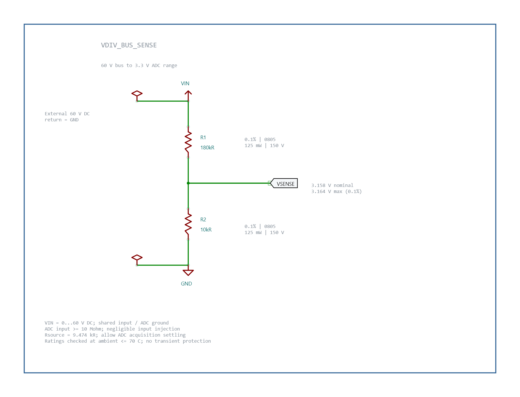
VSENSE = VIN × Rbottom / (Rtop + Rbottom)= 60 × 10 kΩ / 190 kΩ= 3.157895 VHighest initial-tolerance output:60 × 10.01 kΩ / (179.82 kΩ + 10.01 kΩ)= 3.163883 V
| Check | Result | Meaning |
|---|---|---|
| Nominal current | 315.789 µA | Current through the unloaded divider |
| Initial tolerance range | 3.151917–3.163883 V | All four ±0.1% corners; upper limit passes |
| Nominal power | R1 17.950 mW; R2 0.997 mW | Below specified 125 mW rating at ≤70°C |
| Nominal voltage across parts | 56.842 V; 3.158 V | Within respective working-voltage constraints |
| Source resistance | 9.474 kΩ | Must be considered when integrating a sampling ADC |
| 10 MΩ DC ADC load | 3.154906 V nominal | Calculated DC loading |
The nominal simulation reported 3.15789 V and 315.79 µA, matching calculation. All four initial-tolerance corners passed. The component review applied the manufacturer’s lower-of-maximum-voltage-or-√(P×R) working-voltage rule and calculated a conservative 3.170634 V maximum under the stated temperature-drift assumptions. Output, tolerance and resistor-stress checks passed.
Task 26
NTC Sensor: Temperature Points and RC Response
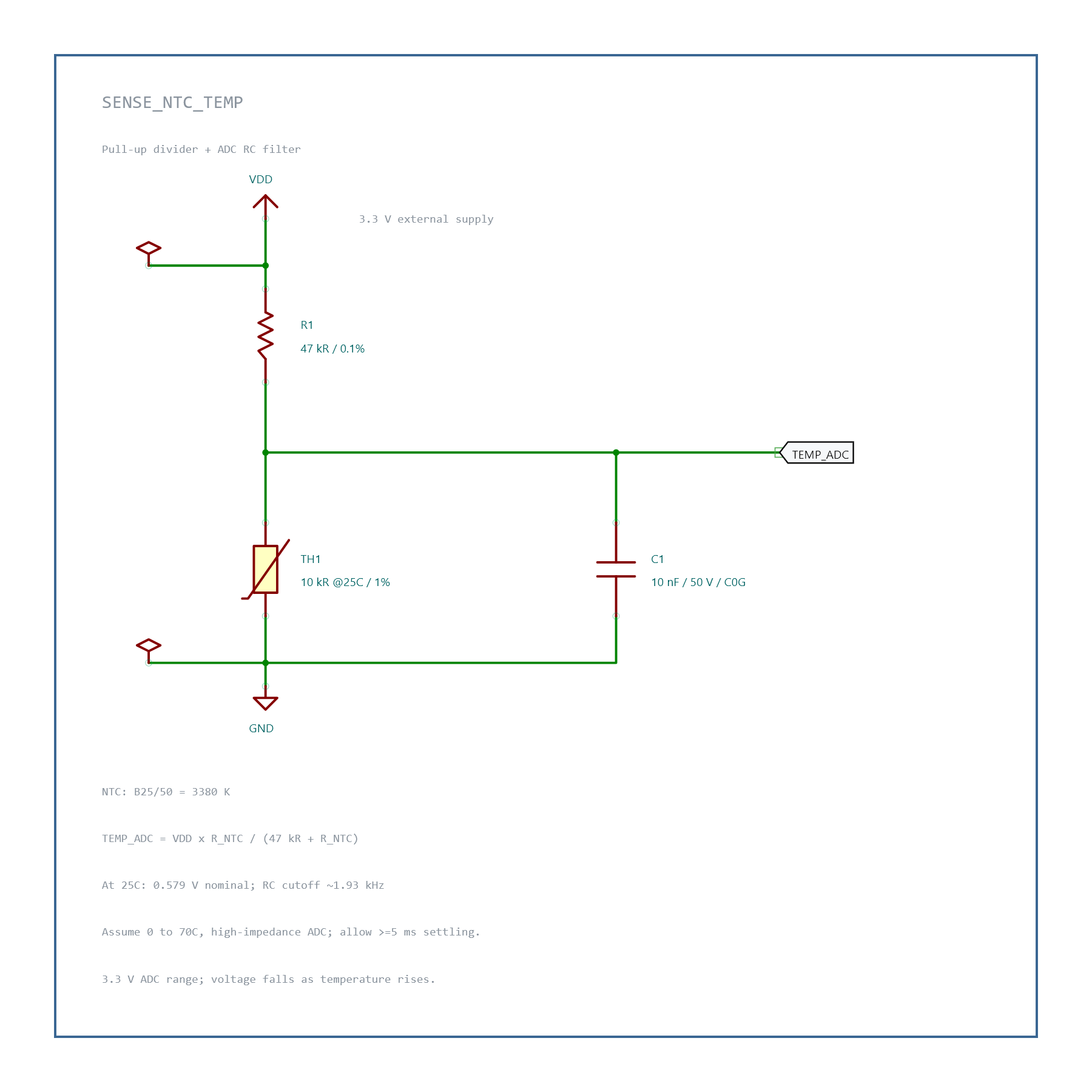
The sensor uses a 47 kΩ ±0.1% pull-up, Murata NCP18XH103F03RB thermistor (10 kΩ at 25°C, ±1%) and 10 nF C0G capacitor from TEMP_ADC to ground, powered from 3.3 V with a high-impedance ADC input. Each temperature test used the corresponding resistance from Murata’s NCPxxXH103 table.
| Temperature | RNTC | Calculated VOUT | Saved simulation | Calculated fc | Electrical τ |
|---|---|---|---|---|---|
| 0°C | 27.219 kΩ | 1.210239 V | 1.210240 V | 923.35 Hz | 172.37 µs |
| 25°C | 10.000 kΩ | 0.578947 V | 0.578947 V | 1.93018 kHz | 82.46 µs |
| 70°C | 2.228 kΩ | 0.149354 V | 0.149354 V | 7.48203 kHz | 21.27 µs |
VOUT = 3.3 × RNTC / (47 kΩ + RNTC)Rsource = 47 kΩ || RNTCfc = 1 / (2π × Rsource × 10 nF)
All three simulated operating points matched the calculations to the reported precision. At 25°C, current is 57.895 µA, estimated thermistor dissipation is 33.52 µW and calculated self-heating is approximately 0.034°C using the typical dissipation constant. The RC cutoff is 1.93018 kHz, with approximately 380 µs electrical settling to 99%. The filter response changes with thermistor resistance, as shown above.
Task 05
LDO Supply: Regulation, Startup and Load Response
The TLV1117-33IDCYR circuit converts 12 V to 3.3 V for a 0–25 mA external load and 0–50°C ambient. Pin 1 is ground, pin 2 and the tab are output, and pin 3 is input. A 560 Ω preload adds approximately 5.9 mA. Input/output capacitors are specified at 22 µF ±20%, rated 35 V and 10 V respectively; the output specification requires at least 10 µF effective capacitance and 0.2–0.5 Ω ESR over operating conditions.
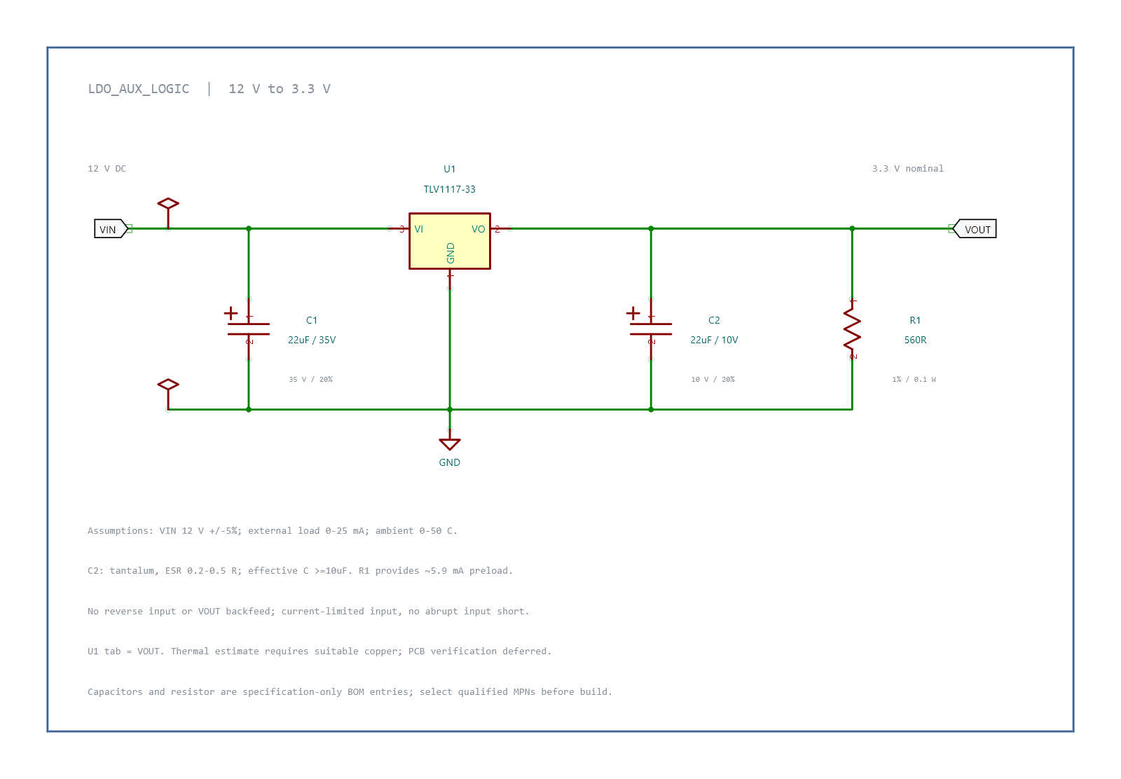
Behavioral-model results
| Test | Measured model result | Interpretation |
|---|---|---|
| 12 V operating point | 3.299073 V; 24.992981 mA external + 5.891203 mA preload | Nominal numerical target passes |
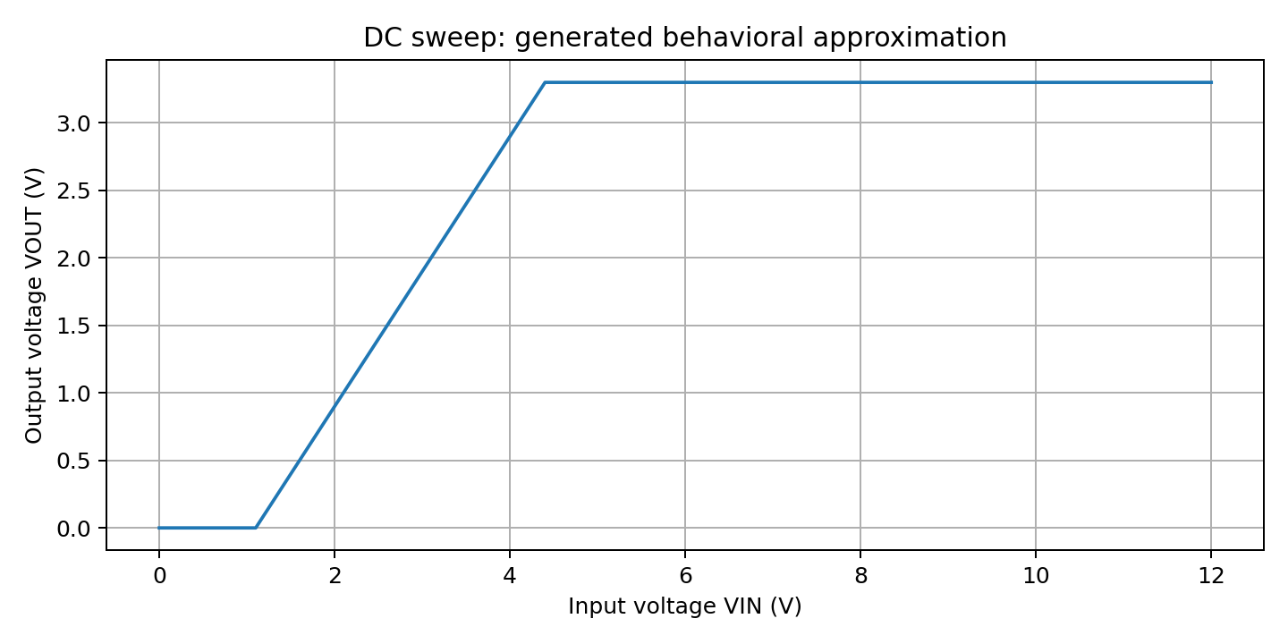
| 0–12 V sweep | Within ±1% at 4.37 V; plateau about 4.40 V | Model headroom: approximately 1.1 V |
| 1 ms input ramp | Enters ±1% at 0.507965 ms absolute; 0.407965 ms after ramp start | No overshoot above 3.3 V in the assumed model |
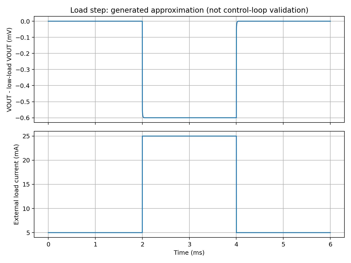
| 5→25→5 mA load | 0.599772 mV loading dip; ~12.85 µs to within 10 µV of new plateau | Behavioral-model load-step response |
Load-step calculation
The model uses an instantaneous 30 mΩ output resistance and 0.3 Ω capacitor ESR. Initial small-signal impedance is 30 mΩ || 300 mΩ = 27.27 mΩ, predicting approximately 0.545 mV for a 20 mA step. The settled change is ΔV = ΔI × Rout = 20 mA × 30 mΩ = 0.600 mV, consistent with the saved result. The audit used 1 µs load edges and 60,020 samples; the reported 12.85 µs recovery is settling to within 10 µV of the new plateau.
Operating-point, input-sweep, startup and load-step checks passed their model targets. Calculated nominal pass-element loss is (12−3.3) × 25 mA = 0.2175 W, or 0.2688 W including preload, before additional bias losses.
Task 33
Voltage Reference: Regulation and Error Allocation
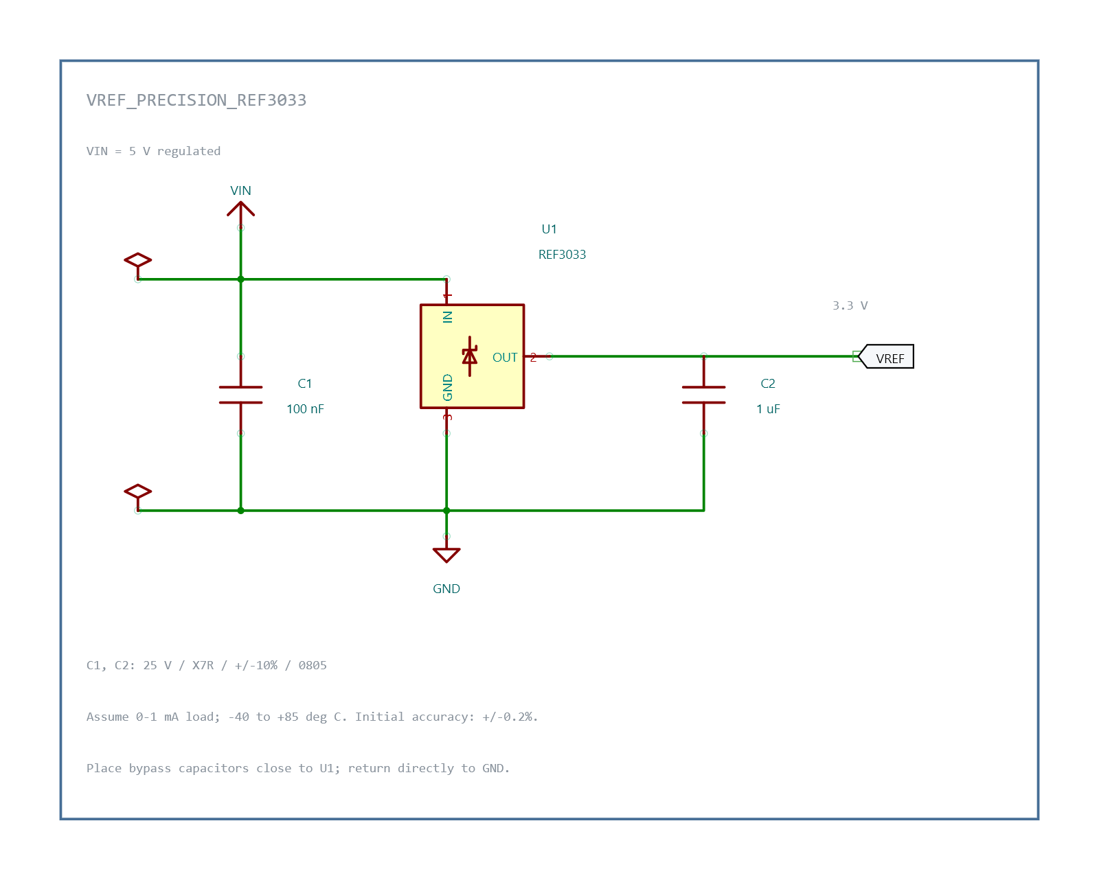
The REF3033AIDBZR circuit derives nominal 3.3 V from 5 V with 100 nF input and 1 µF output decoupling, both specified as 25 V AVX X7R parts. Pin 1 is IN, pin 2 is OUT and pin 3 is GND; OUT connects directly to VREF. The intended source load is 0–1 mA.
Surrogate-model results
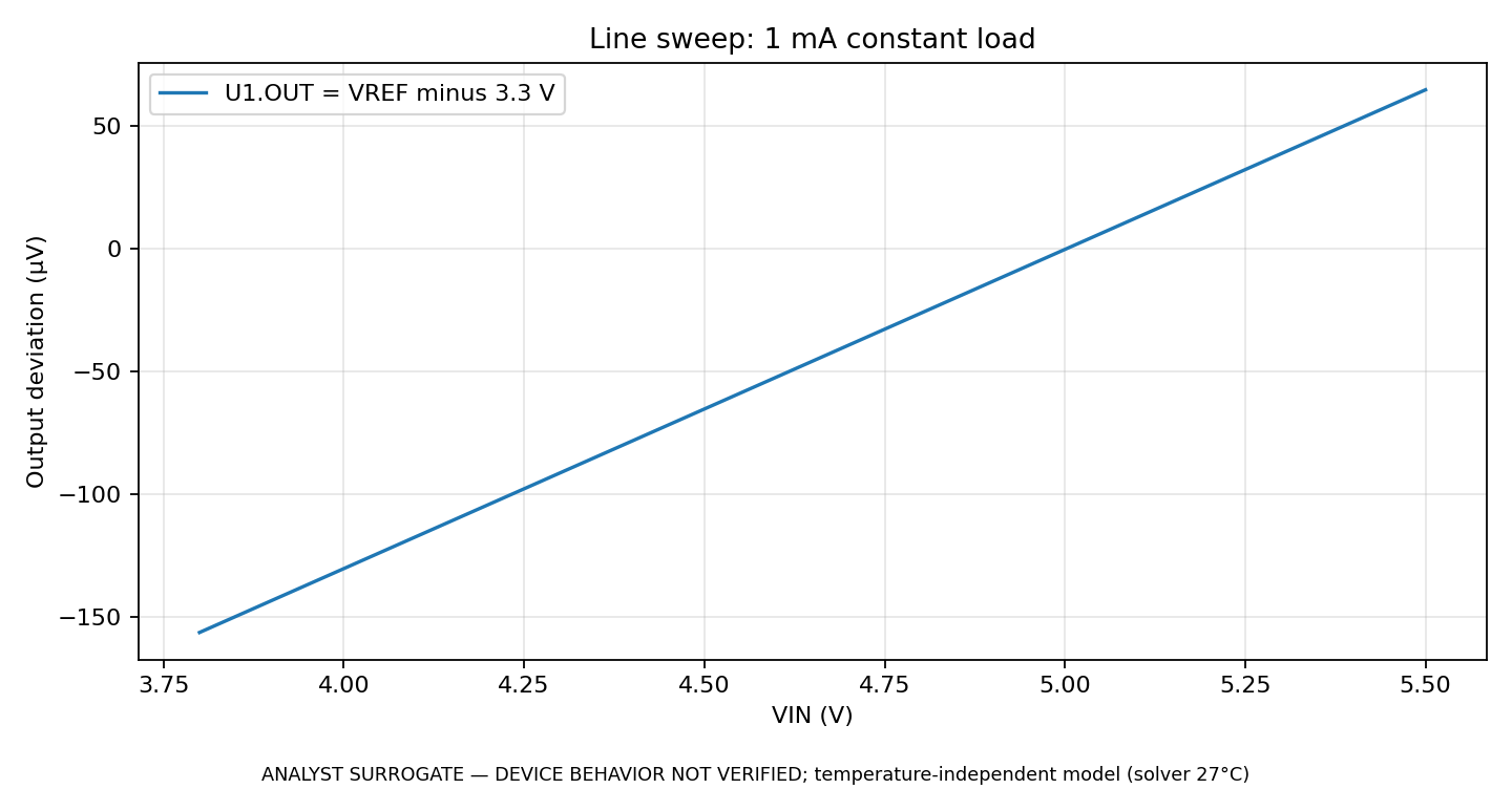
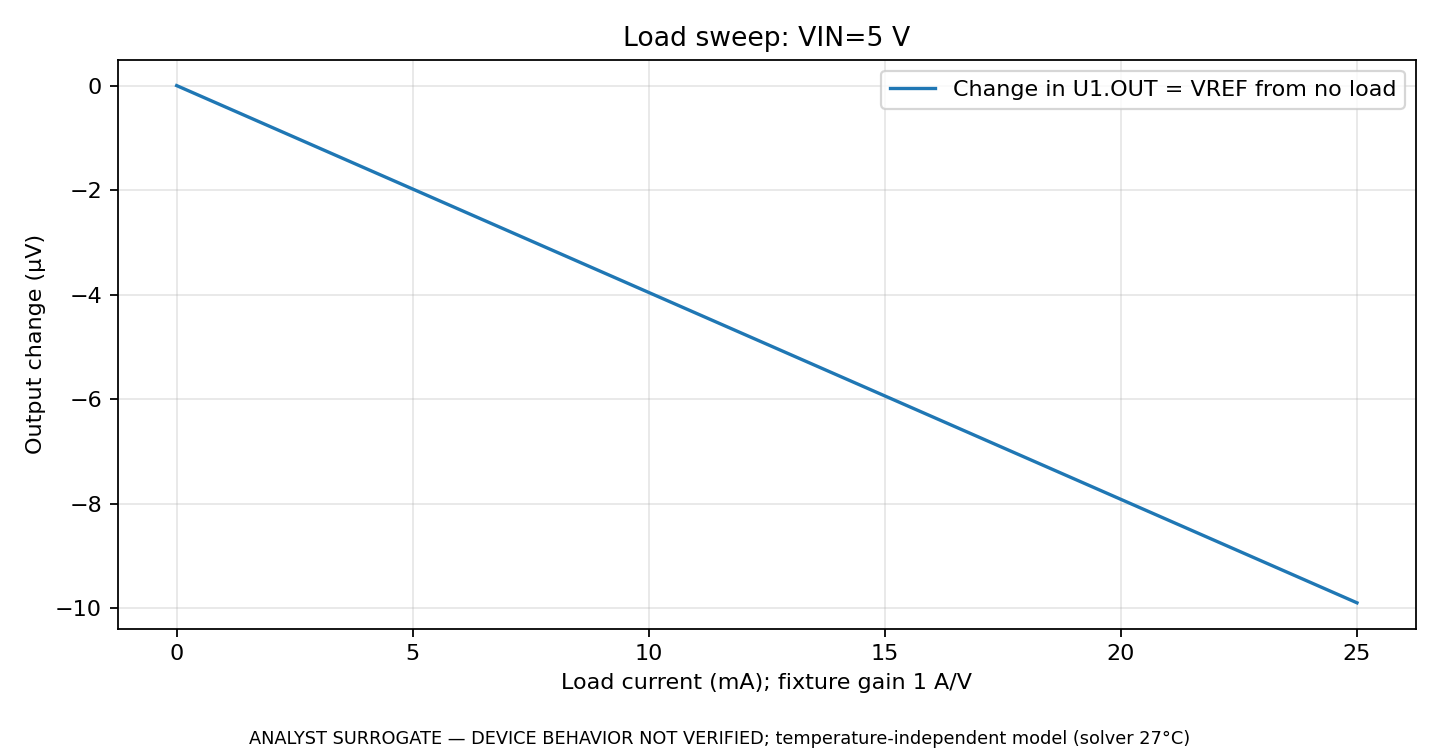
The simulations use REF3033_ESTIMATE_v1_NOT_TI with 3.3 V nominal output, a 130 µV/V line coefficient and 0.396 mΩ output resistance. The regulation sweeps reproduce those model coefficients: 130 µV/V × 1.7 V = 221 µV, and 0.396 mΩ × 25 mA = 9.9 µV. All selected numerical targets passed.
| Test | Saved result | Scope |
|---|---|---|
| 5 V, 1 mA | 3.299999538 V | Nominal surrogate operating point |
| VIN 3.8–5.5 V, 1 mA | 221 µV output span | Reproduces assumed 130 µV/V slope |
| VIN 3.36–5.5 V, no load | 278.2 µV output span | Separate companion run |
| Load 0–25 mA at 5 V | 9.9 µV output decrease | Reproduces assumed output resistance |
| 1 ms supply ramp | 0.840301 ms from t=0; 0.740301 ms after ramp begins to ±0.1% | Surrogate startup response |
Datasheet-based error allocation
| Contribution | Allocation at exactly 5 V | Condition |
|---|---|---|
| Initial accuracy | 6.600 mV | ±0.2% of 3.3 V; nominal 25°C/no-load specification |
| Temperature excursion | 26.8125 mV | 65 ppm/°C ×125°C ×3.3 V; full box-method excursion |
| Load | 0.330 mV | Printed 100 ppm term used in saved report; conditions and unit interpretation noted there |
| Series filter | 0 mV | No physical series component in schematic |
| Conditional total | 33.7425 mV = 1.0225% | Conditional engineering allocation |
The separate accuracy budget uses the full box-method temperature excursion, with no series-filter voltage drop. Its 33.7425 mV total is a conditional engineering allocation across the listed test conditions. Schematic connectivity, decoupling and the original ERC review all passed.
Next steps
Result and next steps
Five selected tasks produced five accepted schematics with supporting connectivity checks, calculations and simulation records. The next step is to extend this evaluation to more complex circuits and physical hardware. No hardware was tested; active-device results shown here are functional or behavioral-model simulations, not measurements of actual chip performance.
Sources
Try ProtoFlow free
Describe a circuit in plain English, import real LCSC/DigiKey/Mouser parts, run DRC/ERC, and export to KiCad, free.
Download ProtoFlow